
 U.S. semiconductor manufacturers are investing hundreds of billions of dollars in domestic fabrication capacity. Driven by surging demand for chips used in artificial intelligence, data centers, automotive systems, and advanced electronics — and supported by federal CHIPS Act funding and state incentives — leading memory and logic manufacturers are constructing new fabs, expanding existing facilities, and building out domestic supply chains at a scale not seen in decades.
This is more than a semiconductor construction story. It is also a long-term advanced-materials supply chain story.
Every new fab requires a dependable supply of precisely specified process gases, chemicals, silicon wafers, specialty metals, sputtering targets, deposition materials, and other manufacturing inputs. High-purity aluminum is an important part of that ecosystem, particularly for physical vapor deposition, semiconductor metallization, bond-pad formation, equipment development, and process research.
What U.S. Semiconductor Expansion Looks Like
Over the past several years, semiconductor manufacturers have announced or broken ground on new fabrication facilities across the United States. Sites in Arizona, New York, Idaho, Ohio, and Texas are among the locations where leading manufacturers are building next-generation logic and memory capacity.
Federal CHIPS Act funding has accelerated these commitments, with billions in direct grants supporting domestic fab construction for manufacturers across multiple product categories. State and local incentives have added further support, and long-term supply agreements for critical materials — including silicon wafers — have been structured to underpin multi-decade production programs.
Together, these projects are expected to create hundreds of thousands of direct and indirect jobs and represent some of the largest manufacturing investments in U.S. history.
A Semiconductor Fab Is Also a Materials Supply Chain
The headline investment numbers are measured in billions of dollars, but a semiconductor fab cannot operate on construction and equipment alone.
Once production begins, fabs require a continuous supply of qualified materials. These materials must meet tightly controlled specifications for purity, dimensions, composition, documentation, packaging, and lot-to-lot consistency.
Materials commonly consumed or used in semiconductor manufacturing include:
● Raw silicon wafers
● High-purity process gases
● Photoresists and specialty chemicals
● Dielectric and barrier-layer materials
● Copper, tungsten, titanium, tantalum, cobalt, and aluminum
● Sputtering targets and evaporation materials
● Quartz, ceramics, and specialized chamber components
The investments major manufacturers are making in domestic wafer supply demonstrate how seriously the industry views the availability of critical raw materials. Long-term supply agreements and investments in domestic production help fabs reduce supply disruption, improve planning, and secure the materials needed for future production.
The same considerations apply throughout the advanced-materials supply chain.
The Role of High-Purity Aluminum in Semiconductor Manufacturing
Aluminum has played a foundational role in semiconductor metallization for decades, and it continues to be used in modern semiconductor manufacturing.
Physical vapor deposition processes create extremely thin, high-purity metal films on semiconductor wafers. Applied Materials identifies aluminum slab metallization and aluminum bond-pad metallization among the most common PVD applications in logic and memory manufacturing.
Within semiconductor and microelectronics production, aluminum may be used for:
● Aluminum metallization and conductive films
● Upper-level metal wiring
● Bond pads that connect a semiconductor die to its package
● Specialized contact and interconnect structures
● Backside and device metallization
● Power semiconductor and sensor fabrication
● Research, process development, and equipment qualification
● Thin-film deposition for advanced electronic devices
Modern semiconductor devices use multiple metals, with each material selected for a particular electrical, physical, and manufacturing requirement. Aluminum remains valuable because of its conductivity, established deposition and etching processes, relatively low resistivity, and extensive history in semiconductor fabrication.
Leading memory manufacturers describe aluminum and copper as metals used to create semiconductor wiring, noting that aluminum remains suitable for certain upper wiring layers where its properties and process compatibility make it the practical choice.
Aluminum Sputtering Targets for PVD
One of the most important forms of high-purity aluminum used in semiconductor manufacturing is the sputtering target.

During magnetron sputtering, plasma ions strike the surface of an aluminum target. Aluminum atoms are released from the target and deposited as a thin film on the wafer or substrate.
This process allows manufacturers to control:
● Film thickness
● Deposition rate
● Electrical performance
● Film uniformity
● Adhesion
● Surface characteristics
● Repeatability from wafer to wafer
Because the target is the source of the deposited material, its purity and physical condition are critical process variables. Semiconductor-focused aluminum targets are manufactured with reduced metallic and gaseous impurities to help limit particle generation during sputtering. Purity requirements commonly begin at 4N, or 99.99%, and may extend to 5N, 6N, or higher for particularly contamination-sensitive applications.
Why Aluminum Purity Matters
In semiconductor production, even trace quantities of an unwanted element can affect a deposited film or introduce an additional variable into a tightly controlled process. For engineers selecting high-purity aluminum, important considerations include:
Verified Chemical Purity
A Certificate of Analysis should document the aluminum purity and relevant trace elements. Detailed elemental analysis may be performed using glow discharge mass spectrometry, commonly known as GDMS, or another appropriate analytical method.
Controlled Metallic Impurities
Elements such as iron, nickel, copper, silicon, zinc, magnesium, and other trace metals may need to be controlled according to the intended deposition process.
Lot-to-Lot Consistency
Once a material has been evaluated or qualified, unexpected changes in its impurity profile can create additional testing requirements. Consistent sourcing and traceable production lots help reduce that risk.
Target Density and Microstructure
For sputtering applications, density, grain structure, surface condition, and internal defects can influence sputtering behavior, particle generation, and deposition consistency.
Dimensional Precision
Target diameter, thickness, flatness, tolerances, backing-plate configuration, and bonding requirements must match the deposition equipment.
Documentation and Traceability
Fabs, equipment manufacturers, laboratories, and process-development teams frequently require lot numbers, Certificates of Analysis, country-of-origin information, and supporting quality documentation.
High-Purity Aluminum Beyond Sputtering Targets
Although sputtering targets are the most direct connection between high-purity aluminum and production-scale PVD, semiconductor organizations use aluminum in many additional forms. These include:
● Aluminum pellets and slugs for electron-beam and thermal evaporation
● Aluminum starting sources for longer deposition runs or larger source requirements
● Aluminum wire and rod for research systems, component development, and specialized fabrication
● Aluminum foil, sheet, and plate for experimental devices, shielding, substrates, fixtures, and custom components
● Aluminum blocks and custom forms for machining, remelting, prototyping, and equipment development
The ecosystem surrounding a major fab includes more than the chip manufacturer itself. Universities, national laboratories, equipment manufacturers, deposition-system developers, packaging companies, component suppliers, and process-research teams all require advanced materials as new technologies move from experimentation to production.
Why U.S.-Based Aluminum Supply Matters
The domestic semiconductor manufacturing buildout illustrates a broader shift toward strengthening U.S. supply chains across the board. Locating fabs in the United States does not eliminate supply chain risk if their essential materials must still travel through long or unpredictable international supply routes.
A U.S.-based high-purity aluminum supplier can offer several practical advantages:
● Shorter and more predictable lead times
● Domestic inventory availability
● Easier communication regarding technical requirements
● Faster access to replacement or development material
● Simplified logistics for small and custom orders
● Lot-specific documentation and traceability
● Support during research, qualification, and production ramps
This is particularly important during process development. Engineers may need several sizes, purity grades, or material forms before identifying the correct specification. Access to in-stock material can help prevent a relatively small material requirement from delaying a larger equipment or research program.
How HPA Supports Semiconductor Research and Manufacturing
High Purity Aluminum is a U.S.-based distributor of 4N through 6N5 aluminum materials for semiconductor manufacturing, PVD, thin-film deposition, research, and advanced manufacturing. Our available products include:
● High-purity aluminum sputtering targets in 4N, 5N, and 6N purity
● Standard disk targets from 2 inches through 12 inches
● Custom target dimensions and configurations
● Aluminum pellets, slugs, and starting sources for electron-beam and thermal evaporation
● High-purity aluminum foil, sheet, plate, rod, wire, coils, and blocks
● Custom aluminum forms and sizes by request
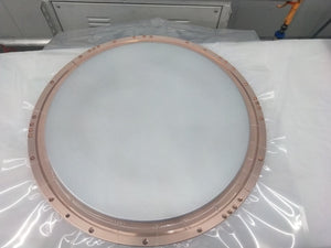
Material is supplied with Certificate of Analysis documentation. Detailed GDMS elemental analysis is available for products and applications requiring lot-specific impurity verification. We work with engineers, researchers, national laboratories, universities, equipment developers, and manufacturers that need the correct aluminum purity, dependable documentation, and responsive U.S.-based supply.
Preparing the Materials Supply Chain for the Next Generation of U.S. Fabs
The scale of domestic semiconductor investment underway is a clear signal that U.S. chip manufacturing is entering a period of sustained expansion.
As new fabs move from planning and construction into equipment installation, process qualification, and wafer production, demand will grow across the supporting materials ecosystem. That includes the high-purity metals and deposition materials used to create, connect, test, and package semiconductor devices.
High-purity aluminum may represent only one part of an extraordinarily complex manufacturing process — but it is an important one. For semiconductor manufacturers, equipment companies, and research teams, securing a dependable source of documented high-purity aluminum can help support process consistency, development timelines, and long-term supply chain resilience.
Are you working in semiconductor manufacturing, thin-film deposition, equipment development, or process research? Contact HPA to discuss your required purity grade, material form, dimensions, Certificate of Analysis, GDMS documentation, and availability.
-> Browse Aluminum Sputtering Targets
-> Browse Aluminum Evaporation Pellets and Starting Sources