Thin film deposition plays a pivotal role across various industries, from semiconductor manufacturing to the production of solar panels. This technology is crucial for applying microscopic layers of materials onto substrates, enabling advancements in electronic devices, optical components, and energy solutions. Central to this process is the use of vacuum coating and sputtering targets, particularly when working with metals, which are fundamental for achieving high-quality, durable coatings.
Understanding Thin Film Deposition
Thin film deposition refers to a range of processes used to deposit layers of material onto a substrate or surface. These processes can be broadly categorized into Physical Vapor Deposition (PVD) and Chemical Vapor Deposition (CVD), each employing different techniques to achieve material deposition. PVD methods, such as sputtering and thermal evaporation, focus on converting the material from a condensed phase to a vapor phase before it condenses on the substrate. substrate.
PVD, or Physical Vapor Deposition, encompasses a variety of vacuum deposition methods, among which sputtering and evaporation are the most prominent. In the sputtering process, ions from an inert gas plasma are directed towards the target material, causing atoms to be ejected from the target's surface and then deposited onto the substrate to form a thin film. This method is highly advantageous for its precise control over film thickness and composition. Thermal evaporation, on the other hand, involves heating the target material until it vaporizes, allowing the vapor to condense on the substrate. This method is particularly valued for its simplicity and efficiency in depositing pure metals and compounds. Both techniques are integral to manufacturing processes requiring uniform, high-quality films with specific properties, highlighting PVD's critical role in advancing thin film technology applications.
CVD processes, meanwhile, involve a chemical reaction occurring on the substrate surface to deposit the material. These methods are particularly significant in the application of metal coatings, due to their efficiency and the quality of the thin film produced.
Chemical Vapor Deposition (CVD) encompasses a set of highly sophisticated techniques crucial for the deposition of high-purity, high-performance solid materials. A typical CVD process involves introducing one or more volatile precursors into the vacuum chamber, where they decompose or react with each other upon the substrate surface, resulting in the desired film. The parameters of the CVD process, including temperature, pressure, and chemical composition, are meticulously controlled to optimize the quality and attributes of the coating. This method is particularly effective for coating complex geometries and is distinguished by its ability to deposit films at comparatively lower temperatures than PVD methods. The versatility of CVD allows for the deposition of a wide range of materials, including metals, oxides, nitrides, and carbides, making it a cornerstone technology in the fields of microelectronics, photovoltaics, and corrosion resistance coatings. Advanced CVD techniques, such as Plasma-Enhanced Chemical Vapor Deposition (PECVD) and Low-Pressure Chemical Vapor Deposition (LPCVD), further refine the process, enabling the production of coatings with exceptional uniformity and conformity.
The choice of deposition method depends on several factors, including the type of material, desired film properties, and production requirements. For example, sputtering is commonly used for metals due to its versatility and ability to produce highly uniform and dense coatings. This makes it ideal for applications such as thin film solar cells and electronic devices. On the other hand, CVD is favored for its ability to deposit high-quality films at lower temperatures, making it suitable for temperature-sensitive materials and delicate substrates.
The Role of Metals in Thin Film Deposition
Metals are commonly utilized in thin film deposition for their electrical, optical, and physical properties. Materials such as gold, silver, copper, and aluminum are used to enhance the functionality and performance of devices. The selection of a specific metal or alloy depends on the desired outcome of the thin film coating, including considerations such as conductivity, reflectivity, and adherence to the substrate.
Metals such as gold, silver, copper, and aluminum play a critical role in enhancing the functionality and performance of various devices through thin film deposition. Gold, admired for its excellent electrical conductivity and resistance to corrosion, is often used in high-reliability electronic applications. Silver, with the highest electrical and thermal conductivity of all metals, is vital for RFID tags, OLEDs, and conductive inks. Copper, favored for its outstanding electrical conductivity and thermal transfer capabilities, is essential in semiconductor devices and integrated circuits, ensuring efficient power distribution and heat dissipation.
Among these metals, aluminum stands out for its unique combination of properties, making it a particularly versatile choice for thin film applications. Notably, aluminum offers excellent conductivity, affordability, and is lightweight, with a lower atomic mass compared to other metals like gold and copper. This makes it an attractive option for electrical conductors, capacitors, and reflective coatings. Aluminum's natural oxide layer provides an inherent resistance to corrosion, which can be further enhanced through anodization, a process that thickens this protective layer. Furthermore, aluminum's ability to form alloys with other metals increases its utility in thin film deposition, allowing for the adjustment of its physical properties to meet specific performance criteria. The preparation and deposition of aluminum require careful control to avoid oxidation and ensure the purity of the deposited film. Techniques such as sputtering or e-beam evaporation in a controlled vacuum environment are typically used to achieve high-quality aluminum coatings, which are critical for applications ranging from packaging materials to optical components and mirrors.
The purity of aluminum used in thin film deposition plays a crucial role in determining the performance and reliability of the end product. For applications requiring high conductivity and corrosion resistance, such as in microelectronics and photovoltaic cells, aluminum of 99.99% purity (4N) or higher is typically employed. This level of purity ensures minimal presence of impurities that could compromise electrical performance or lead to increased oxidation, potentially affecting the film's integrity and functionality. In more demanding applications, such as in advanced semiconductor devices, the requirement for aluminum purity can be even more stringent, with specifications calling for 99.999% purity (5N) or higher. At these elevated purity levels, the control of trace elements becomes critical, as even minute amounts of contaminants can significantly impact the electrical properties and thermal behavior of the deposited films. Achieving such high purity levels necessitates sophisticated refining processes prior to deposition and rigorous control of the deposition environment to prevent contamination. This underscores the importance of selecting the appropriate aluminum purity level based on the specific requirements of the application to ensure optimal performance of the thin film coating.
Vacuum Coating Technologies for Metals
Vacuum coating technologies, including sputtering and thermal evaporation, are essential for depositing metal thin films. These PVD techniques operate under vacuum conditions to prevent contamination and ensure the uniformity of the deposited films. Sputtering involves bombarding a target material with ions to eject atoms that then deposit on the substrate. Thermal evaporation, on the other hand, heats the coating material until it vaporizes and condenses on the substrate. Each technique offers distinct advantages for metal coatings, influencing factors such as film purity, density, and adhesion.
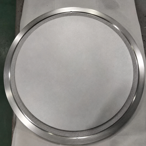
Sputtering Targets in Metal Thin Film Deposition
Sputtering targets are crucial components in the deposition process, serving as the source material for the thin film. The choice of target material, purity, and shape significantly impacts the deposition outcome. For metal coatings, targets are available in various configurations, including planar and rotary designs, to accommodate different sputtering systems. The selection of sputtering targets involves considering factors such as target-to-substrate distance, deposition rate, and the intended application of the coated surface.
Innovations in Metal Thin Film Deposition
Recent advancements in thin film deposition technologies have focused on improving the efficiency, quality, and reliability of metal coatings. Automation and control solutions are being developed to enhance the precision of deposition processes, while new sensing technologies monitor film thickness and uniformity in real time. These innovations are poised to drive the future of metal thin film deposition, offering improved outcomes for industry applications.
Case Studies and Applications
The application of metal thin film deposition spans diverse sectors. In the semiconductor industry, metal coatings are essential for fabricating integrated circuits and chip components. Solar panels benefit from metallic thin films that improve light absorption and conductivity. Additionally, medical implants utilize biocompatible metal coatings to ensure longevity and functionality. These real-world examples underscore the versatility and importance of vacuum coating and sputtering targets in thin film deposition.
Conclusion
Vacuum coating and sputtering targets are indispensable for achieving high-quality metal thin films, contributing to advancements across multiple industries. By selecting appropriate deposition methods and materials, manufacturers can enhance the performance and durability of their products. The ongoing development of thin film deposition technologies promises to further expand the potential applications of this field.
To explore the latest in thin film deposition and vacuum coating technologies, consulting with industry experts can provide valuable insights tailored to specific project needs. Engaging with these advancements is crucial for leveraging the benefits of metal thin films in today's technological landscape.